

The Indian government has formally notified Semicon 2.0, a ₹1,27,500 crore semiconductor programme aimed at expanding the country’s chip manufacturing and design ecosystem.
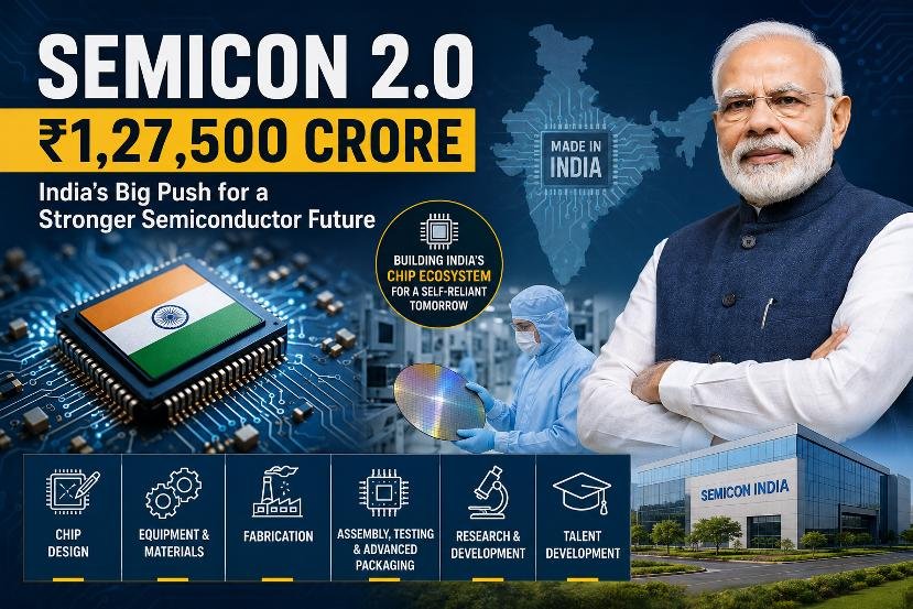
The scheme, notified on August 31, 2026, broadens government support beyond semiconductor fabrication to cover chip design, advanced packaging, manufacturing equipment and materials, research and development, and talent development. The government says the initiative will help build a robust and resilient semiconductor ecosystem in India.
What Is Semicon 2.0?
Semicon 2.0 is the second phase of India’s semiconductor programme and is designed to support the industry across the wider value chain.

The programme has been organised around six key pillars:
- Semiconductor chip design
- Semiconductor equipment and materials
- Semiconductor fabrication
- Assembly, testing and advanced packaging
- Research and development
- Talent development
The government has issued notifications covering all six pillars, with the India Semiconductor Mission overseeing implementation.
Focus Shifts Beyond Chip Fabs
A major feature of Semicon 2.0 is its broader approach to semiconductor manufacturing.
Under the scheme, silicon semiconductor fabs can receive fiscal support equivalent to 40% of eligible capital expenditure, while compound semiconductor, display and certain specialised fabs can receive support of up to 35%.
Advanced ATMP and OSAT packaging projects are eligible for support of up to 35% of capital expenditure, while conventional or legacy packaging projects can receive up to 25%.
The programme will also support semiconductor design companies, equipment manufacturing and materials production, helping India develop capabilities across multiple stages of chip production.
Government to Identify Strategic Chips
Electronics and IT Minister Ashwini Vaishnaw has said a high-level expert panel will identify strategic semiconductor products that could qualify for incentives.
The panel will be jointly chaired by the Principal Scientific Adviser and the National Security Adviser, with strategic importance and national priorities expected to guide the selection process.
This could allow government support to be directed towards chips considered important for sectors such as electronics, telecommunications, automobiles, defence and other strategic industries.
Boost for Domestic Semiconductor Capabilities
Semicon 2.0 is intended to reduce India’s dependence on overseas semiconductor supply chains while strengthening domestic design, manufacturing and packaging capabilities.
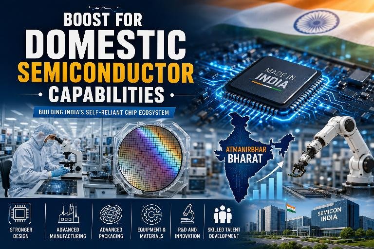
The government is also placing greater emphasis on semiconductor research and skilled talent. Reports on the programme indicate that India aims to train an additional 100,000 semiconductor design engineers over the next five years.
Why Semicon 2.0 Matters
Semiconductors are critical components used in smartphones, automobiles, computers, telecommunications equipment, defence systems and other advanced technologies.
With its ₹1,27,500 crore fiscal outlay, Semicon 2.0 aims to position India as a stronger participant in the global semiconductor value chain by supporting chip design, fabrication, packaging, equipment, research and skilled manpower.